Focussed Ion Beam (FIB)
A focussed ion beam or FIB operates in a similar way to an SEM. While an SEM uses a beam of electrons to image and analyse samples, a FIB uses an energetic beam of ions such as Ga+ to image, ablate, analyse, pattern and deposit materials.
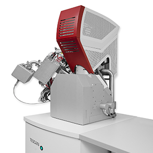
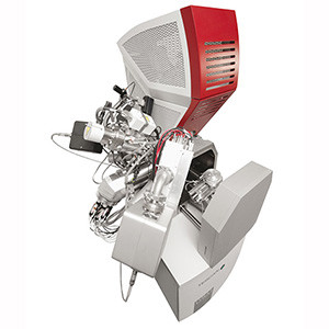
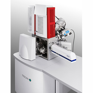
Dual Beam Systems
FIBs have become popular for materials and biological applications where they are used with an integrated SEM column. This setup is known as a dual beam system.
How Does a FIB Work?
Milling or surface ablation can be achieved using a high current beam of Ga+ ions. When the ions strike the sample surface, a small amount of material is sputtered. The removed materials leaves the surface in the form of secondary ions or neutral atoms. This process is capable of machining surfaces with nananoscale precision.
At low beam currents almost no material is removed from the sample surface and the focussed, the ion beam can be used for imaging. In this mode it can achieve resolutions of the order of 5nm.
FIB Imaging
FIB imaging has two modes of operation, secondary electrons and secondary ions. Both of these are produces by the ion beam and offer advantages over more conventional SEM imaging.
FIB secondary electron imaging produces images with extreme grain orientation contrast, eliminating the requirement for chemical etching.
FIB secondary electron imaging also finds specific application in life sciences in the form of correlative fluorescent microscopy. This is possible as the ion beam does not interact with the signals from fluorescent probes used to label proteins.
FIB secondary ion imaging is particularly useful for corrosion studies as it is able to reveal chemical differences as secondary ion yields of metals can increase by three orders of magnitude in the presence of oxygen.
Applications of FIBs
FIBs were originally used for semicondustors ..
They are now finding use in:
- Micro and nanomachining
- Ion beam induced deposition or FIB-assisted CVD
- Semiconductors
- Preparation of TEM samples
- Cross-sectional SEM imaging
- In-situ electrical characterisation at the nanometer scale
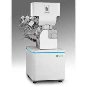
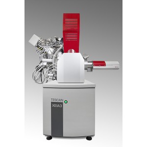
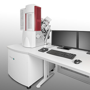
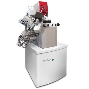
Products
![]()