Microanalysis – Enhancing Electron Microscopy with Chemical Analysis
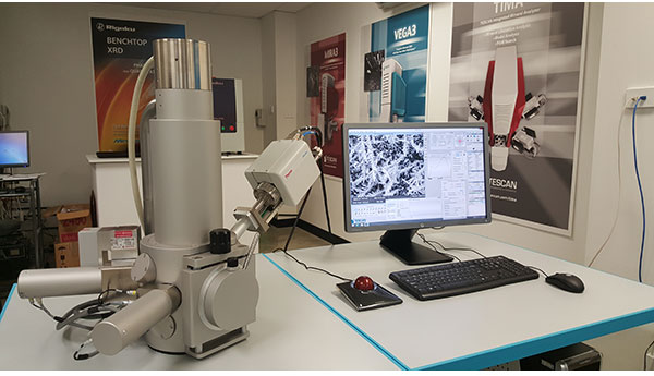
Scanning Electron Microscopes
The invention of the Scanning Electron Microscope (SEM) brought with it significantly better resolving power compared to any microscope that came before it, with magnifications up to 1,000,000X now possible. It also opened the door to high spatial resolution chemical analysis which adds another invaluable dimension for materials analysis.
Weve all seen some of the cool micrographs and images generated by an SEM. These images provide us with detailed structural information about your sample. This can be augmented with chemical information, similar to micro XRF (X-Ray Fluorescence) mapping to show elemental concentrations and distributions. Correlating the structural and chemical data gives us a much better understanding of the system being investigated.
Chemical Analysis in SEM
SEM chambers are now built to take any number of detectors that measure emissions of various natures that tell us more about the samples we are investigating. Microanalysis techniques like EDS (Energy Dispersive Spectroscopy) and WDS (Wavelength Dispersive Spectroscopy) provide elemental information and are extremely useful in materials development and failure analysis. In this article we compare these two techniques and their relative advantages and disadvantages.
More recently, the addition of an ion beam column or FIB (Focussed Ion Beam) to an SEM opens up yet more possibilities in the area of chemical analysis. Using TOF-SIMS (Time of Flight Secondary Ion Mass Spectroscopy), researchers have greater freedom, with the ability to accurately detect all elements from the periodic table, in particular light elements as well as isotopes. Herein, we contrast ToF-SIMS with EDS and WDS.
Using techniques like those listed above gives the microscopist similar analytical capabilities to a chemist using techniques such as mass spectrometry, AAS (Atomic Absorption Spectroscopy) or even XRF. However, unlike the former two, the sample does not need to be digested and can potentially be examined using other techniques if required.
Energy Dispersive Spectroscopy (EDS) and Wavelength Dispersive Spectroscopy (WDS)
EDS and WDS will be discussed together as they have several similarities and a comparison is provided at the end of this section.
How They Work
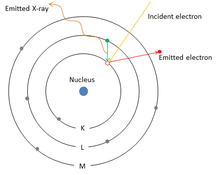
Figure 1. Schematic showing the interaction of incident electrons and the resultant generation of characteristic X-ray.
The basic operating principle of both EDS and WDS is the same and is analogous to energy dispersive and wavelength dispersive XRF (X-Ray Fluorescence), with the exception EDS and WDS use electrons and EDXRF and WDXRF use X-rays to dislodge electrons from the sample.
The physics behind both EDS and WDS is identical. In both cases electrons from the EM column dislodge electrons from the electron shells of atoms in the sample. As electrons are ejected from these atoms, they leave vacancies that are filled by electrons that fall down from higher energy electron shells. In doing so, they emit energy in the form of X-rays. These X-rays are of a characteristic energy native to the atom or element that they have evolved from. Furthermore, by measuring the intensity of X-rays at a particular energy level, the relative concentration of that element can be determined.
EDS
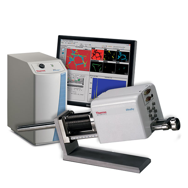
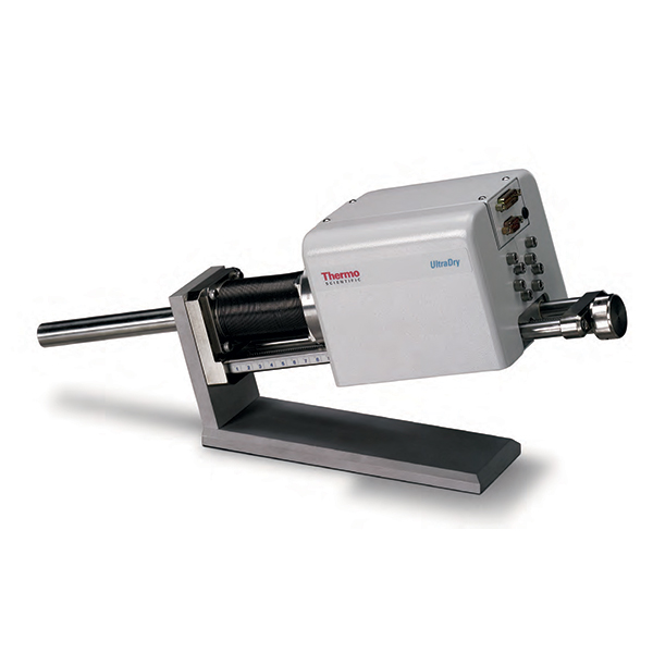
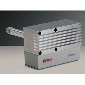
EDS has been around for a long time. Earlier systems were based in Si(Li) crystals and needed liquid nitrogen cooling. Modern systems like the Thermo Scientific UltraDry utilise the latest technology Silicon Drift Detectors (SDD) that do not require liquid nitrogen cooling and offer much higher count rates, resulting in faster analyses.
WDS
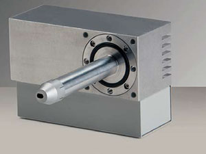
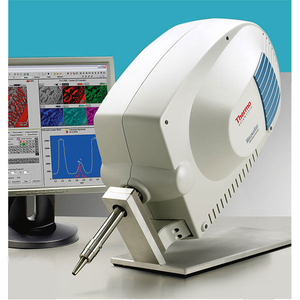
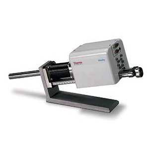
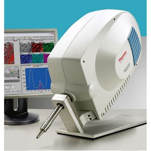
WDS detectors like the Thermo Scientific MagnaRay are the latest evolution incorporating the latest technology and operate in a very similar fashion to an EDS detector. The difference is EDS can capture a full spectrum simultaneously, whereas the spectra for a WDS is captured sequentially. In comparison, WDS is significantly slower, although it produces more accurate results with an improved signal to noise ratio and more clearly resolved peaks.
Comparison
The typical characteristics of EDS and WDS spectrometers are compared in table 1.
Table 1. Comparison of EDS vs WDS.
| EDS | WDS | |
|---|---|---|
| Detectable elements | Z≥4 (Be) | Z≥4 (Be) |
| Resolution | Energy dependent (~130eV at 5.9keV | Crystal dependent (~5eV) |
| Signal to Noise Ratio (Relative) | Lower | Higher |
| Spectral Artefacts | Typically include escape peaks, pulse pileup, electron-beam scattering, peak overlap, and window absorption effects | Almost none |
| Ability to detect trace elements (Relative) | Lower | Higher |
| Relative data collection time | Faster | Slower |
| Relative cost | Lower | Higher |
Figure 2 shows the spectra of monazite containing rare earth elements. This clearly demonstrates the difference in data produced using both techniques i.e. the clearly resolved peaks and significantly improved signal to noise ratio.
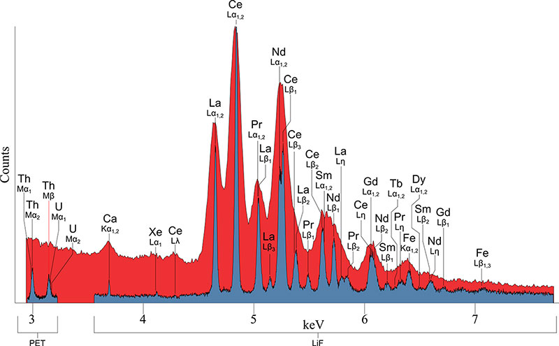
Figure 2. EDS (red) and WDS (blue) spectra for a rare earth containing monazite sample.
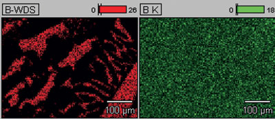
Figure 3. WDS (left) and EDS (right) maps of boron (<3%) in steel .
The resolving power of WDS is further exemplified in mapping applications (figure 3) where it is clearly able to show elemental distributions of trace elements. In contrast EDS is unable to provide the same level of detail.
EDS is the more commonly used technique probably on account of its faster speed and cheaper capital cost. However, when higher levels of accuracy are required, especially the ability to detect trace elements, WDS comes into its own. That all said, the accuracy of EDS is still very good and suitable for most applications.
Purpose-Designed Systems Based on EDS
 EDS is inherently a time-consuming analytical technique. Utilising multiple EDS detectors can reduce analysis times as well as removing shadow and geometrical effects. Bespoke systems like the TESCAN TIMA-X (TESCAN Integrated Minerals Analyser) employ four EDS detectors and are designed to provide high-throughput analysis of mineral samples.
The TIMA-X is an automated solution with fully integrated hardware and software working seamlessly together to generate information about phases present, phase distributions and associations and liberation analysis. Based on the elemental composition, the system is able to determine what minerals are present and in what concentrations as well as a host of other relevant information.
The data produced by the TIMA-X can be fed back directly into the processing environment to optimise throughput and efficiency of mining or minerals processing operations. The ability to perform large area mapping and generate data in near real-time makes it an ideal solution for industrial applications.
ToF-SIMS
ToF-SIMS provides elemental analyses like EDS and WDS, but goes further and is able to also generate chemical state and molecular information. As such, it can discriminate isotopes and molecular compounds including polymers, organic compounds as well as amino acids and is able to detect all elements, including light elements. This has enabled it to be used for research into lithium ion batteries which is not possible using EDS or WDS.
In comparison to EDS and WDS, it is also much more surface sensitive generating data from the top surface (typically 1nm) of solid materials. This makes it more suitable for the accurate analysis of thin films. It also has better spatial resolution, typically better than 0.1µm
How Does TOF-SIMS Work?
A finely focused beam of ions such as Ga or Cs, typically generated by a FIB column impinges on the surface of a sample. As a result, secondary ions and ion clusters are emitted from the surface. By accelerating these species into a specially designed Time-of-Flight analyser, the mass of the emitted ions and clusters can be determined by measuring the time it takes for them to reach the detector. Emitted species have the same kinetic energy, but with differing masses, heavier species take longer to reach the detector compared to lighter ones. Using this and the intensity of the SIMS peaks, the chemistry of the element or molecular fragment can be determined.
Due to the fact that the flight time can be measured down to the nanosecond, TOF-SIMS has a mass resolution as fine as 0.00X atomic mass units (i.e. one part in a thousand of the mass of a proton). It also does not discriminate against any materials with a mass in the range of 0 to 10,000amu.
Furthermore, by rastering the beam, maps of the sample surface can be produced. The beam can also be used to ablate the surface allowing depth profiling to be accomplished.
Using powerful computers, ToF-SIMS are able to reference back every pixel so that detailed (2D) maps and 3D reconstructions can be generated based on mass spectra collected.
ToF-SIMS vs. EDS/WDS
Table 2. Comparison of ToF-SIMS to other microanalysis techniques (EDS/WDS).
| Advantages of ToF-SIMS | Disadvantages of ToF-SIMS |
|---|---|
| • Better detection of light elements (down to H) • Much better mass resolution • Depth profiling • Better spatial resolution • The ability to distinguish isotopes, ions and molecular compounds • Can be used on organic materials e.g. tissue samples for biological research • More surface sensitive • Non-destructive | • Can only generate semi-quantitative results • Sample charging (can often be overcome using charge compensation routines) • Large amounts of data (full spectrum/pixel) can result in long acquisition times |
Applications of ToF-SIMS
To date, most ToF-SIMS applications are in the area of materials science. However, with increasing awareness, it is also broadening its appeal and infiltrating other areas. Some examples of where it is being used include:
- Polymers
- Pharmaceuticals
- Semiconductors
- Geology
- Coatings and thin films
- Catalysts
ToF-SIMS Integration
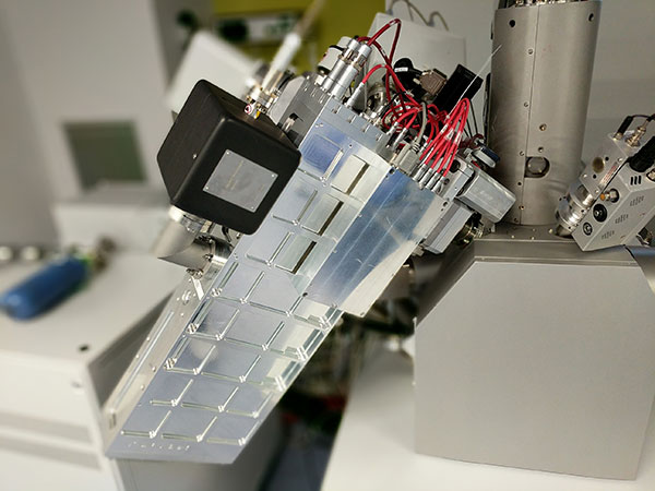
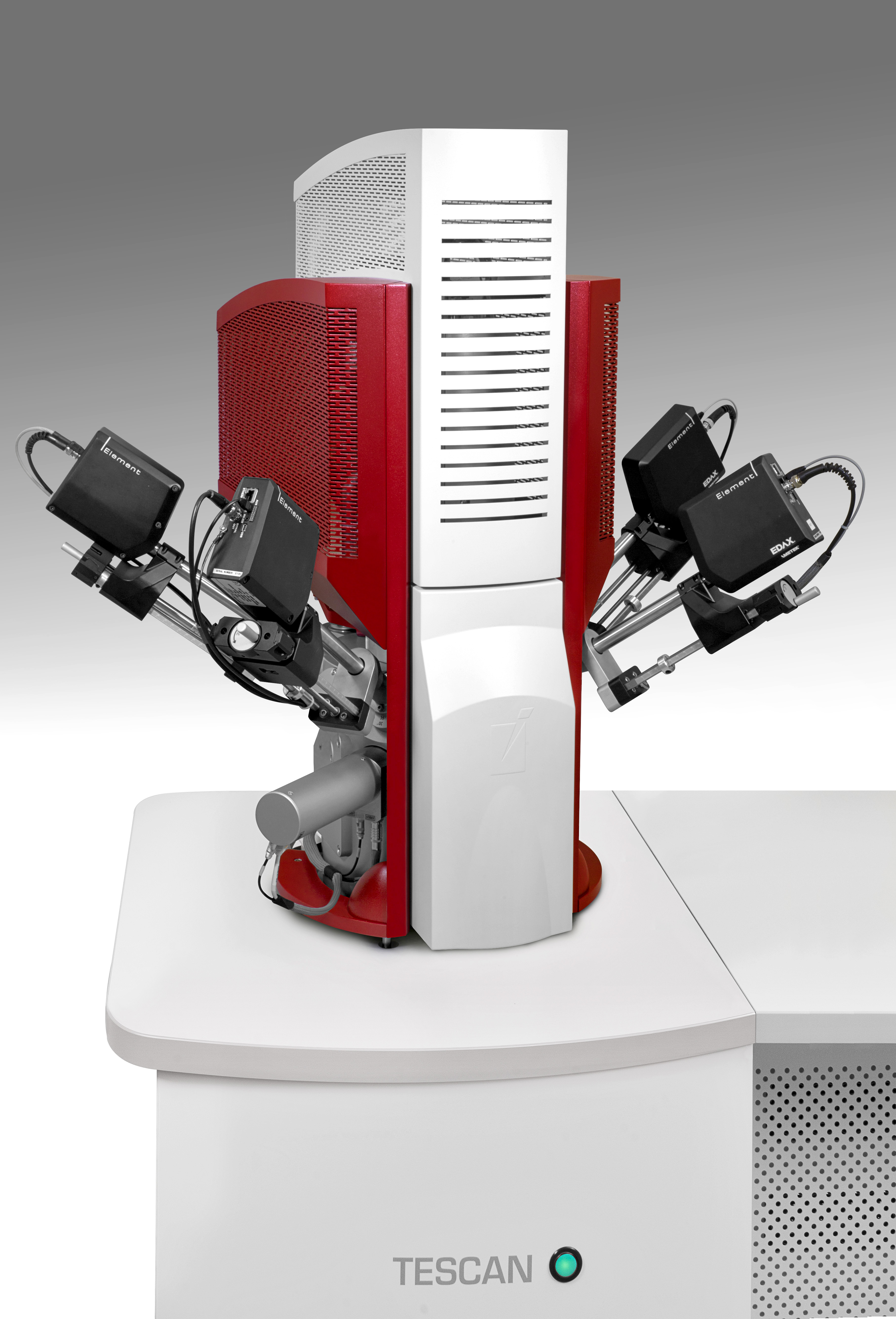
Figure 4. ToF-SIMS detector integrated into TESCAN FIB-SEM.
TESCAN are the first SEM or FIB-SEM manufacturer to develop a fully integrated system with ToF-SIMS. Using a system from TOFWERK (Switzerland), TESCAN are able to integrate the ToF-SIMS with any of their conventional (Gallium) or Xe-plasma FIBs (figure 4). These systems also have the ability to add several other detectors for added analytical capabilities as well as being ideal for producing TEM lamellae.
Summary
Elemental analysis or microanalysis is a highly important tool for electron microscopists increasing their analytical power and helping to generate more in depth understandings of the systems they are investigating. Compared to EDS and WDS, ToF-SIMS is the new kid on the block. It is also a more evolved sibling, able to provide more information, with increased accuracy and versatility, with the ability to measure any element and any isotope as well as organic species. Furthermore, when paired or integrated with a FIB, it is able to generate detailed 3D chemical reconstructions making it an extremely powerful tool for materials analysis.
This is a modified version of the article “Enhancing Electron Microscopy with Chemical Analysis” published in Materials Australia, June 2017.