
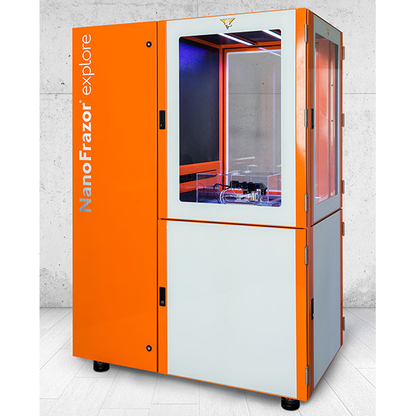
NanoFrazor Explore Rapid Prototyping System for Nanostructures and Nanodevices
The NanoFrazor Explore is a unique tool designed specifically for the nanofrabrication of structures and patterns at the nanoscale. Its simple operation allows researchers to quickly produce high resolution nanosized geometries in a single step with unparalleled precision and accuracy and is suited to a wide range of applications.
Operating Principle
Most nanopatterning devices use Electron Beam Lithography or E-Beam Lithography. These systems use a focused beam of electrons to mill shapes and patterns into the surface of a material covered in an electron-sensitive material or resist.
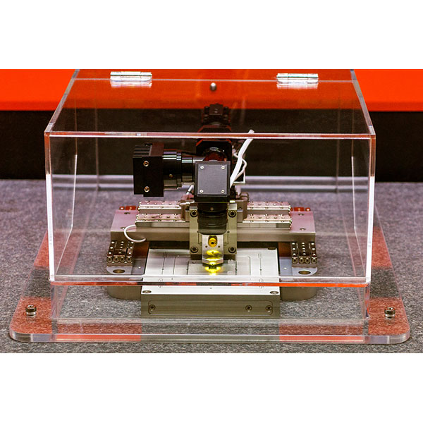
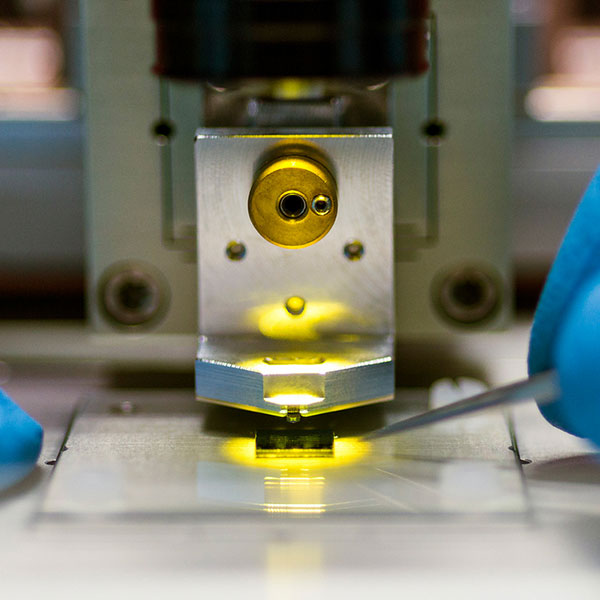
The NanoFrazor on the other hand uses thermal Scanning Probe Lithography (t-SPL) technology. This employs a sharp tip mounted on a silicon cantilever, much like an AFM. By heating the tip using an integrated microheater, localised heating of an organic thermally responsive resist results in selective and controlled decomposition into volatile species which evaporate. This makes the fabrication of nanosized features possible.
t-SPL technology has many advantages over EBL. Click here for more details.
Resolution
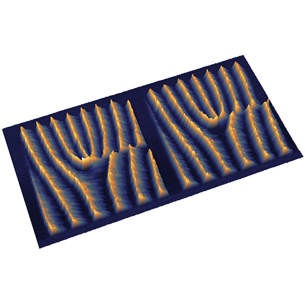
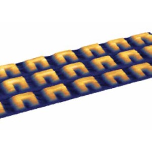
The nanopatterning resolution of the NanoFrazor is limited by the size of the tip. As an example, the SLhp-09 tips can be smaller than 10nm at the apex. The nanosized features produced approach the dimensions of the tip itself.
The system has successfully produced well-separated, well defined parallel lines 3.5nm deep, with a pitch of 20nm.
Speed
High scan speeds are ensured with the purpose-designed piezo positioning system. This system also provides high positioning accuracy and next to zero out-of-plane movement across the entire scan range.
The cantilevers have an integrated electrostatic actuation mechanism. This provides fast and controlled vertical movement of the tip which is a prerequisite for high-speed patterning.
Closed Loop Lithography
The Closed Loop Lithography methodology utilised in the NanoFrazor Explore make it extremely robust. The system also provides simultaneous inspection of the written pattern which in turn provides the operator with instantaneous feedback and quality control on the process.
Simultaneous inspection reduces both fabrication and subsequent inspection timeframes compared to other nanolithography techniques.
Key Features
Key Features of the NanoFrazor Explore include:
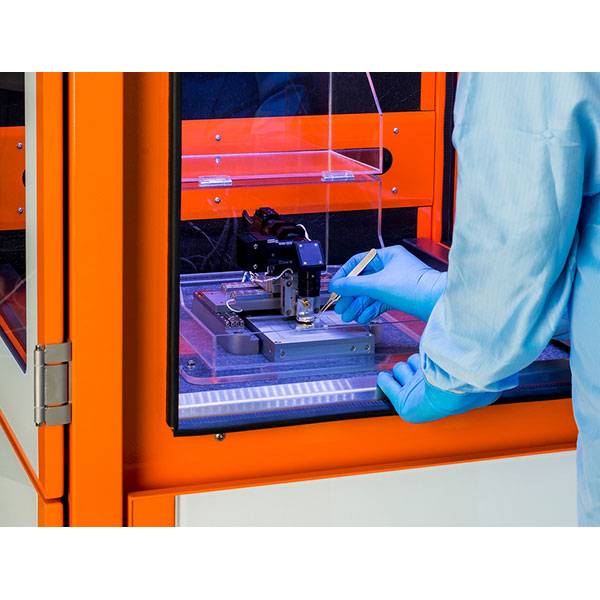
- area accessible by the tip 100 x 100mm
- Modes Write, Read or write+read (CLL mode)
- Correlation stitching
- Correlation overlay
- Integrated high resolution optical microscope
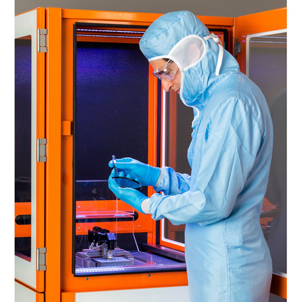
- Simple cantilever exchange
- User-friendly graphical user interface providing access to all basic functions
- Open software platform allowing user customisations (based on C++ and Igor Pro)
- Triple layer anti-acoustic housing
- Vibration isolation granite table with threads and space to mount additional equipment
- Integrated 19 rack allow with room for additional controllers
- Integrated gas supply making it independent of the lab environment
- Humidity and temperature monitoring
- Casters for easy relocation
- Small footprint 127.5 x 77.6cm
- Attractively priced to suit tight university and R&D budgets
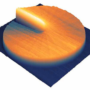
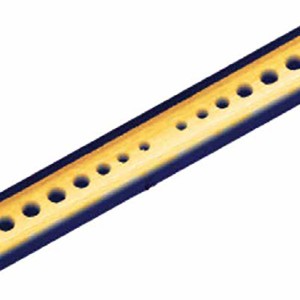
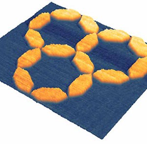
Applications
Nanophotonics
3D optical elements like spiral phase plates, microlenses or holograms.
Nanophotonics
Photonics crystals, cavities or waveguides with low roughness.
Plasmonics
High resolution metal structures for metamaterials or optical antennas.
Nanoelectronics
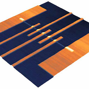
Novel nanowire and quantum devices using precise overlay.
Nanomagnetism
Smaller magnetic structures for studies on spintronics or artificial spin ice.
Stamps & Moulds
Unique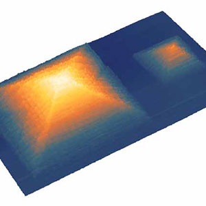 Unique precision with 3D templates for NIL or injection moulding.
NanoFrazor Explore uses thermal Scanning Probe Lithography (tSPL) that has several advantages over other techniques such as E-Beam Lithography. These advantages are summarised in the following table.
| thermal Scanning Probe Lithography | E-Beam Lithography | |
|---|---|---|
| Resolution Half-pitch demonstrated | <10nm | <10nm |
| Write Speed @10nm resolution | ~1mm/s | ~1mm/s |
| In situ Inspection with <1nm vertical resolution | Yes | No |
| 3D Nanolithography with <2nm vertical accuracy | Yes | No |
| Closed-Loop Lithography Combining patterning & inspection | Yes | No |
| Correlation Overlay Marker free with <5nm accuracy | Yes | No |
| Correlation Stitching Natural surface roughness as marker | Yes | No |
| Chemical Patterning Local heating of various materials | Yes | No |
| Wet development necessary & critical for the pattern | No | Yes |
| Electron damage possible with graphene, nanowires etc | No | Yes |
| Proximity corrections dose adjustment necessary | No | Yes |
| Atmosphere Inside the system | Ambient/Nitrogen | UHV |
| Maintenance repeated effort & cost | Cantilever Exchange ~1 min, $60, every few days | Service Contract ~$30,000 pa excluding parts |
| Energy Consumption, Voltage of the whole system | <1kW, 10V | >10kW, 100kV |
| Footprint & Room Requirements for good usability & performance | <2m2, any room | >10m2, shielded clean room |
| Publication Potential | Very High New technology only commercially available since 2014 | Low Technology is >50 years old and has been widely used |
Nanofabrication by Thermal Scanning Probe Lithography – Webinar