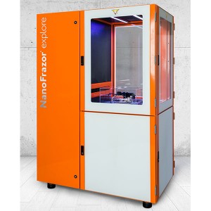
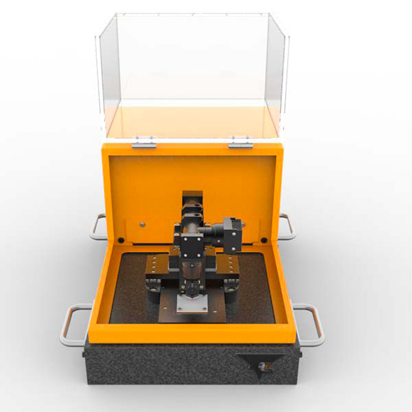
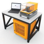
NanoFrazor Scholar – Rapid Nanofabrication System for Producing 3D Nanopatterns
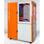
The NanoFrazor Scholar is rapid nanofabrication system for producing nanopatterns. It the smaller sibling to the Nanofrazor Explore that was first introduced to the market in 2014. It benefits from all the same thermal scanning probe lithography (t-SPL) technology with in situ closed loop AFM as its bigger brother, but is small enough to sit atop a bench.
The NanoFrazor Scholar provides a convenient lower cost entry point into t-SPL technology, while still offering rapid prototyping capabilities for producing 3D nanostructures. The small footprint also enables the system to fit inside a glovebox for processing under controlled atmospheres if required.
Key Features
- Direct-write greyscale nanolithography
- In-situ inspection provides additional topography information and accuracy
- No electron damage to sensitive materials
- Precise overlay & stitching capabilities based on imaged topography
- Intuitive and easy to use software interface
- Automatic tip temperature calibration, surface detection and approach
- Low maintenance cost
- Operates in ambient/nitrogen atmosphere
 Thermal Scanning Probe Lithography (t-SPL)
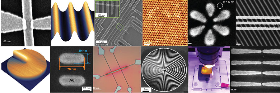
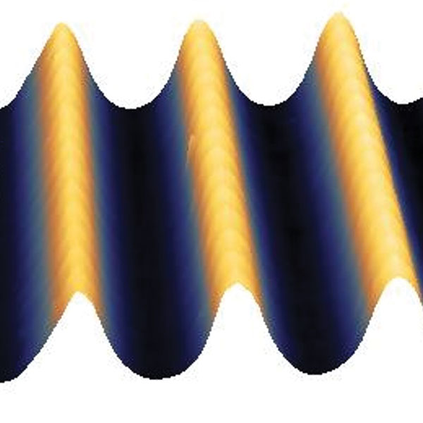
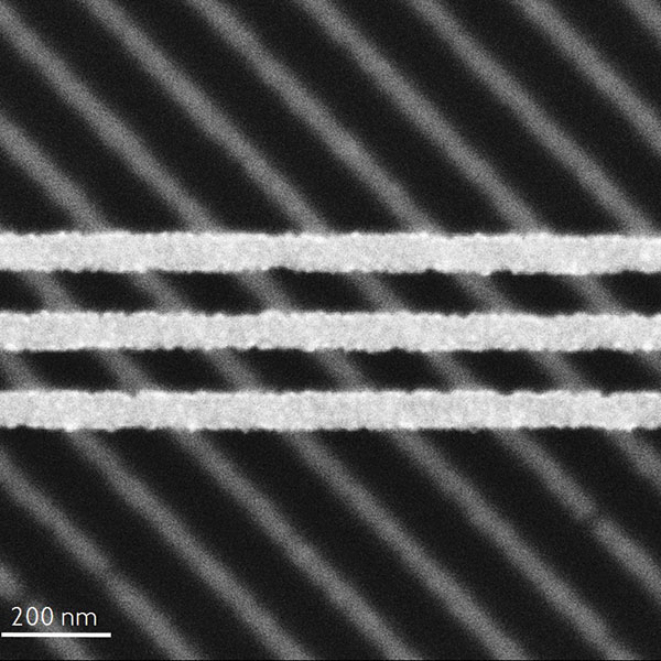
t-SPL is an evolutionary step beyond Electron Beam Lithography (EBL), a technology that has been around for over 50 years. Like EBL, t-SPL can be used for the rapid prototyping of nanostructures where it can be used to produce structures with nanoscale geometries.
t-SPL uses a sharp tip like an AFM tip mounted onto a silicon cantilever. The tip is heated using an integrated microheater to produce localised heating. When used in conjunction with a suitable organic thermally responsive resist, selective and controlled decomposition takes place resulting in the evaporation of volatile species and fabrication of nanosized features.
Advantages of t-SPL
t-SPL has two major advantages over EBL:
- It can be performed in ambient conditions, negating the need for ultra high vacuum conditions
- It incorporates an AFM with simultaneously measures the sample as it is being fabricated
Other advantages of t-SPL can be found by clicking here for more details.

| Nanofrazor Scholar | Nanofrazor Explore | |
|---|---|---|
 |  |
|
| Sample | ||
| Max. sample size X,Y,Z (mm) | 30, 30, 10 | 100, 100, 20 |
| Substrate material | No restrictions (transparent, conducting, magnetic...) | No restrictions (transparent, conducting, magnetic...) |
| Patterning | ||
| Lateral patterning resolution (feature size and half-pitch in resist) (nm) | <30 | <25 |
| Vertical (3D) patterning resolution (distinguishable step size in resist) (nm) | <3 | <2 |
| Topography Imaging | ||
| Lateral imaging resolution (topography feature size) (nm) | <10 | <10 |
| Vertical imaging resolution (topography sensisitivity) (nm) | <0.3 | <0.3 |
| Overlay & Stitching | ||
| Stitching accuracy (nm) | <30 | <20 |
| Overlay accuracy (nm) | <30 | <20 |
| Scanner | ||
| Scan range Z scanner (µm) | 15 | 20 |
| Scan range XY scanner (µm) | 50 x 50 | 75 x 75 |
| Resolution of positioning sensors (nm) | <0.3 | <0.15 |
| Scan speed (during patterning and imaging @ 30 nm pixel size) (mm/s) | 0.5 | 1.0 |
| Long Range Positioning System | ||
| Travel range (X,Y,Z) (mm) | 30, 30, 15 | 100, 100, 25 |
| Resolution of positioning sensor (nm) | <150 | <5 |
| Travel speed (mm/s) | 20 | 20 |
| Optical Microscope | ||
| Resolution (diffraction limit of optics) (µm) | 3.6 | 2.4 |
| Field of view (mm) | 1.3 x 1 | 1.3 x 1 |
| Environment Control | ||
| Damping quality of vibration isolation (vertical & horizontal) | Vibration isolation not included | > 98 % @ 10 Hz, resonance < 1.5 Hz |
| Housing | ||
| Footprint (cm) | 50 x 32 (excl. controller) | 128 x 78 |
| Height (cm) | 30 (excl. external controller) | 185 |
| Weight (kg) | 100 | 650 |
| Upgrade Options | ||
| Trade-in upgrade to NanoFrazor Explore | Possible | Not applicable |
| IntegratedLaserWriterUnit | Not possible | Yes (under development) |
| Multi-tip cantilever operation (chip with up to 10 cantilevers) | Not possible | Yes (under development) |