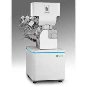
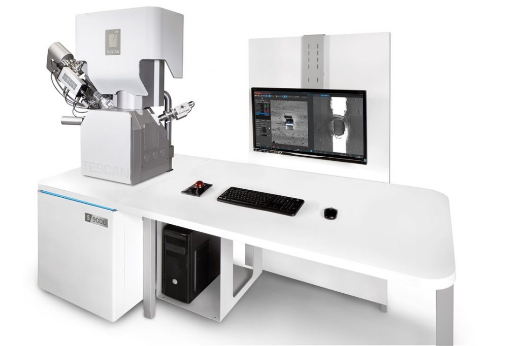
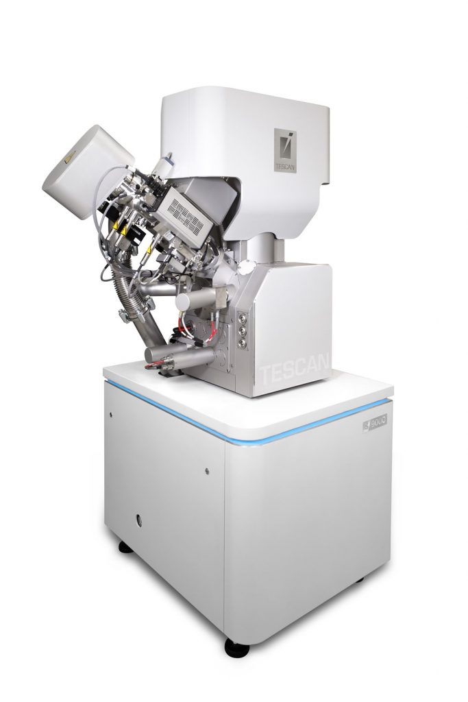
S9000X Xe Plasma FIB-SEM with Superior Resolution and Milling Speed
The S9000X plasma FIB-SEM is suited to the most challenging nano-applications requiring the highest levels of precision and throughput
The S9000X is TESCANs next generation Xe plasma FIB-SEM combining ultimate levels of resolution with the highest FIB milling rates for high throughput sample preparation and characterisation. These capabilities make the S9000X the ideal system for high precision characterisation of nanosized structures.
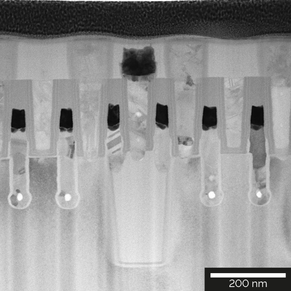
The new Xe plasma FIB (iFIB+) provides precise, damage-free large area cross-sectioning perfect for 3D sample characterisation and rapid TEM lamellae preparation. In conjunction with TESCANs next generation TriGlav ultra-high resolution SEM column, the S9000X is your ideal partner for analysis of the most challenging nanomaterials.
Key Features
- New Essence user interface – Provides easier, faster, and smoother operations, including collision model and customisable, application-oriented layout
- Next generation Triglav UHR SEM column– for ultimate resolution and superb performance at low beam energies and optimised In-Beam detection system
- Energy-filtering axial electron signal collection – for enhanced surface sensitivity
- New iFIB+ Xe plasma FIB column with unmatched FoV– enabling extremely large-area cross-sectioning
- New generation of SEM In-lens detection – combined with high sputtering rates for ultra-fast 3D microanalysis
- Proprietary gas chemistry and recipes –for physical failure analysis of packaging technologies and IC planar deprocessing
- Precise piezo-driven beam aperture changer– enables fast switching between FIB pre-sets
- Strip with 30 FIB apertures – results in extended lifetime and minimum maintenance
- Semi-automated spot-optimising wizard– simplifies selection of FIB milling conditions
- Dedicated workflow-oriented SW modules – wizards and recipes maximum throughput and make FIB access easier for users of any experience level
Why Xe Plasma FIB?
Xe plasma FIBS are able to achieve very high ion beam currents up to 2µA with out compromising beam quality. Furthermore, thanks to continuous developments, small, high precision probes with resolution better than 15nm can are possible at 30keV. This combination of power and precision make the iFIB+ the ideal tool for large scale milling.
Compared to Ga FIBs, inert Xe plasma offers a number of advantages:
- No (Ga) ion implantation and hence no alteration of physical properties
- Less amorphous damage caused
- Wider range of ion beam currents available
- Up to 50x faster milling speeds
- Large FIB currents for fast milling with no need for gas enhancement
- Highly localised and controlled sample modification and nanoengineering
- No formation of intermetallic compounds
- Xe ions enhance detection limits of ToF-SIMS analysis
- Shortest time-to-data, improving throughput
These factors make Xe plasma FIBs a superior alternative to Ga FIBs for TEM lamellae preparation and the ideal companion for 3d microanalysis techniques such as EBSD and ToF-SIMS.
Key Benefits
- Extremely high-throughput milling rates The Xe plasma FIB column can generate extremely high FIB currents (up to 2µA) while maintaining a high precision spot. This permits high speed, high precision milling.
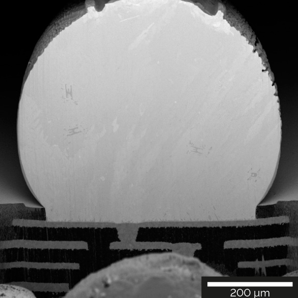
- Unmatched FoV suited to extremely large area cross-sectioning Boasting the largest FoV of any plasma FIB-SEM (1mm at 30keV) and ultra-high sputtering rates 1mm wide cross-sections can be achieved quickly
- Versatile FIB analysis and microengineering large ion beam current range enabling a range of applications e.g. high currents for rapid milling and fast material removal, medium currents for FIB-tomography and low currents for TEM lamellae polishing and delayering and ultra-low currents for damage-free polishing and nanopatterning
- High performance gas injection system The new OPTIGIS is a fast and efficient gas injection system, essential for FIB operations. The S9000Xcan be equipped with up to 5 OPTIGIS units or an inline multi-nozzles 5-GIS system. Proprietary gas mixtures and recipes can also be used
- Maximum precision and performance The new iFIB is driven by an ultra-stable HV supply and precise piezo-driven beam aperture changer that allows rapid switching between FIB presets. The semi-automated spot optimizing wizard allows you to easily select the optimal spot size youre your specific FIB milling application
- Robust detector system The system can collect SE and BSE signals across the entire take-off angle range gathering the most information possible using the TriSE and TriBE detectors
- Minimal surface damage and modification Xe plasma eliminates the possibility of ion implantation and also minimizes the chance of amorphous damage. Xes inert nature also negates the formation of intermetallics which can alter the properties of the sample
- Optimised imaging The next generation Triglav columns in-beam detection system provides significantly improved detection efficiency. With extended detection capabilities, energy-filtered axial BSE signals can now be collected enhancing surface sensitivity selectively collecting low-energy axial BSEs
- Enhanced surface sensitivity and meaningful contrast The Triglav column gives users complete control of surface sensitivity with the option to explore at different contrasts. The S9000X can acquire both signals simultaneously for better insights into your sample. Resolution at low and ultra-low beam energies resolution using Beam Deceleration Technology
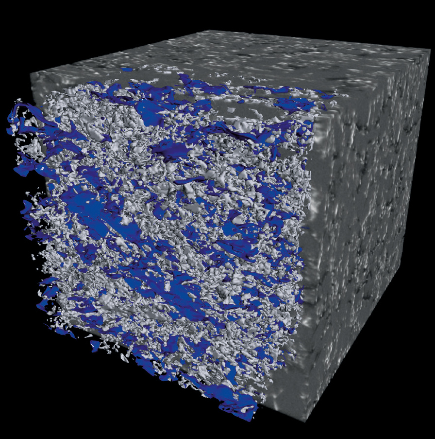
- Ultra-fast 3D microanalysis The new, enhanced in-lens detection system enables fast imaging at high sputtering rates, with ultra-fast data 3D EDS and EBSD collection rates. Furthermore, EDS and EBSD signals can be collected while FIBing, while post processing software can carry out 3D reconstructions on all manner of samples
- Optimised conditions for microcroanalysis The Triglav column alco comes with adaptive spot shape for improved resolution at high beam currents. Tgis is ideal for fast EDS, WDS and EBSD analysis
- Improved ToF-SIMS detection limits Enhanced detection for integrated ToF-SIMS with no interference from Ga peaks which can interfere with Ce, Ge and Ga)
- Fast microanalysis with no sacrifice of spatial resolution The Triglav SEM column features a new Schottky FE gun capable of beam currents up to 400nA and rapid beam energy changes. Direct and continuous control of the beam spot size and current using real time In-Flight Beam Tracing guarantees the best conditions for microanalysis
- Simplified operation The new TESCAN Essence software interface is a simplified multi-user interface with a layout manager that enables fast and easy access to the functions your require. The system is easy to learn and can be tailored to suit your specific application. In-built modules, wizards and recipes bring complex operations well within the reach of novice users boosting both productivity and the usage of higher end functionalities helping to justify your expenditure. The included DrawBeam function also facilitates fast and precise FIB milling and Electron Beam Lithography
- Large wafer analysis The large chamber has been optimized for analysis of 6 and 8 wafers at any location