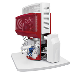
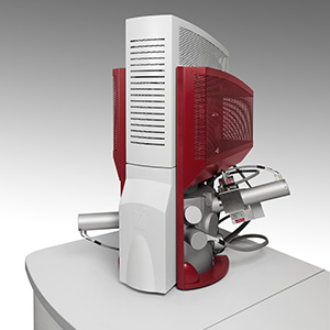
Scanning Electron Microscopes – SEMs
A scanning electron microscope is a type of electron microscope that images samples by scanning them with a focused beam of electrons. This gives them the ability to produce magnifications of up to 500,000 times. This compares to optical or light microscopes that can achieve magnifications of 1000 times.
Light microscopes use white light as the illumination source. White light uses light in the range 400-700nm. Based on the average wavelength of 550nm, the theoretical limit of resolution is approximately 200-250nm. The significantly shorter wavelength of electrons offers a much better resolution compared to white light. The resolution of an SEM depends on numerous factors such as electron spot size and sample interaction volume with the electron beam. This leads to resolutions in the order of 1nm.
How Does an SEM Work?
In an SEM electrons are generated at the top of a column. They are accelerated towards the sample via a combination of electromagnetic lenses and apertures. The lenses and apertures produce a fine focused beam of electrons. The source of electrons, or the way in which electrons are produced defines a number of different types of SEMs. Of these, thermionic and Field Emission Gun (FEG) are the most common.
The electron beam rasters across the sample surface. The electrons themselves interact with the surface atoms to produce various signals that can in turn be detected using specifically designed detectors to provide information about topography and composition.
To be imaged in an SEM, samples must have electrically conducting surfaces. If the specimen is electrically insulating it will need to be coated in carbon or gold to provide a conductive coating. The purpose of the conductive coating is to avoid the accumulation of electrostatic charge.
Imaging Environments
SEMs generally require samples to be held under vacuum to be able to be imaged. It is possible to use a low vacuum, wet environment for biological samples.
With the right hardware, it is also possible to image samples at temperatures from cryogenic to elevated temperatures.
Thermionic SEMs
Conventional SEMs use an electron beam that is thermionically emitted from an electron gun that incorporates either:
- A tungsten filament – Tungsten is used due to its high melting point, low vapour pressure and low cost
- Lanthanum Hexaboride (LaB6) Source This common high-brightness source produces a brightness 5-10 times that of a tungsten filament and offers superior lifespans.
Field Emission Gun (FEG-SEM)
FEG-SEMs come in two varieties:
- Cold Cathode Type – These use very sharp single crystal tungsten tips under an extremely large electric field which causes the cathode to emit electrons via the tunneling effect. They however, use the field emission to produce the electron beam. The sharp tip results in improved emission and focusing ability.
- Thermally Assisted Schottky Type This type employ a tungsten tip coated with a zirconia (ZrO2) layer which increases the electrical conductivity at high temperatures.
Compared to thermionic sources, FEGs:
- Produce finer electron beams compared to thermionic electron guns
- The electron beam is more coherent
- The current densities and hence brightness is as much as three orders of magnitude greater resulting in improved signal to noise ratios and spatial resolution
- Have much greater emitter lifespans
Signals
The interaction of the electron beam and the sample generates signals including:
- Secondary Electrons (SE)
- Back-scattered Electrons (BSE)
- Characteristic X-Rays
- Cathodoluminescence (CL)
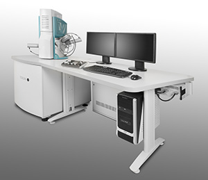
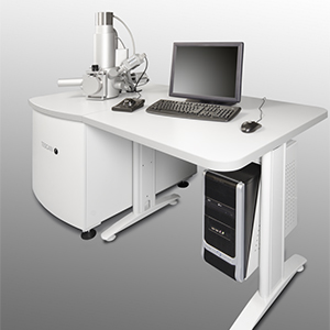
Related Products

![]()