XPS – X-Ray Photoelectron Spectroscopy for Surface Characterisation
XPS or X-ray photoelectron spectroscopy is the most broadly applicable analytical technique used to characterise surfaces. At its heart it determines what elements are present and in what proportions, and hence can be used to determine stoichiometry. It is also able to identify and quantify what chemical state an element is present in and therefore the chemical structure can be deduced, making it a very powerful analytical tool.
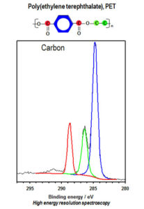
Figure 1. Selected area spectra for PET showing three different chemical states for carbon.
The surface of a material is extremely important as this is the part of a component that actually interacts with its surroundings, and in almost all cases will be the first part to wear, corrode or fail. In addition, the outermost surface may behave differently to the bulk of the material, making an understanding of its properties all the more critical.
With increasing importance being placed on the surface, a clear understanding of this region can enable components to be engineered to be non-wetting, resist corrosion, bond better, have increased catalytic activity and as a result perform better and potentially increase the efficiency of an overall process. It may also be that it is only the outermost extremities, perhaps a few atomic layers, that are important, and hence surface sensitive techniques are required for an accurate characterisation.
XPS used to be a technique that was used only by surface scientists with systems resembling metallic porcupines. However, with surge in popularity of surface engineering, functional and optical coatings, catalysts, sensors etc., XPS has also grown in popularity. While perhaps not as commonplace as XRD, and not producing sexy images like SEM, it is nevertheless increasing in relevance, providing data and an understanding of surfaces that is almost impossible by any other technique.
In recent times, XPS is being used to characterise anything and everything with a surface. It is used for high end research as well as industrial and engineering applications looking at everything from non-stick frypans to solar cells, from fabric coatings to graphene (touted as the latest wonder material). The evolution of the technique, through hardware, software and other technological developments has also helped grow the popularity and versatility of XPS.
Origins of XPS
XPS revolves around the photoelectric effect which was first reported by German physicist Heinrich Hertz in 1887, but was unable to explain it. However, it was not until well after Wilhelm Rontgen discovered X-rays (1895), Albert Einstein explained the photoelectric effect (1905) and several other scientific discoveries that the first high-resolution XPS spectra was collected by Swedish physicist Kai Siegbahn and his team. This happened in 1954, although he and his team preferred to call the technique Electron Spectroscopy for Chemical Analysis or ESCA.
In 1967 Siegbahn published a comprehensive volume that explained the versatility of XPS and its potential application to inorganic and organic materials. The first commercial XPS was produced by Hewlett-Packard under his leadership just two years later. His pioneering work on XPS earned him a Nobel Prize in Physics in 1981.
Other Surface Sensitive Chemical Analysis Techniques
XPS differs from other surface sensitive techniques such as FTIR and Raman in that it provides elemental analyses as opposed to the latter which determine molecular species present on the surface. Secondary Ion Mass Spectroscopy (SIMS) is probably the next closest technique to XPS for surface analysis. It uses energetic ions to bombard the surface as opposed to X-rays. It is more sensitive to trace quantities than XPS, but the data is harder to quantify.
How Does It Work?
Without launching into a detailed physics lesson, a sample is exposed to an X-ray beam. The X-ray knocks electrons out of the surface. By counting these electrons and measuring their energies, XPS is able to determine what elements are present in the surface and their relative quantities. A more detailed explanation of the technique and the physics can be found at www.xpssimplified.com.
XPS generates data from the top 1-10nm of a sample and is suitable for any material from metals, through to polymers, ceramics and composites as well as such things as semiconductors, biomaterials and biologicals. This level of sensitivity is matched by only a handful of other analytical techniques.
It is sensitive to all elements with the exception of hydrogen and helium, with concentrations as low as parts per thousand able to be detected.
An XPS spectrum is essentially a plot of the number or electrons ejected (Y axis) versus their binding energy (X-axis). Elements present can be determined as each species has characteristic spectral peaks that correspond that elements electron configuration.
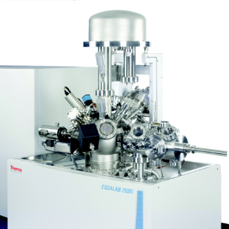
Hardware
An X-ray photoelectron spectrometer consists of the following main components:
- Ultra-High Vacuum Chamber Keeps the system free of contaminants and allows a longer photoelectron path
- X-ray source Typically aluminium anodes that emit Al k? radiation (photon energy 1486.6 eV) and often fitted with a monochromators to improve energy resolution for better spectral information.
- Flood Gun Essential for analysing polymers and insulating materials. It counteracts the build up of charge as a result of electrons leaving the surface. Without it, meaningful data would not be collected for non-conductive samples.
- Transfer Lens Focusses and slows photoelectrons emitted by the sample onto the electron energy analyser for improved detection and measurement.
- Analyser A hemispherical sector energy analyser (HAS)
- Ion Gun For cleaning and milling surfaces for depth profiling
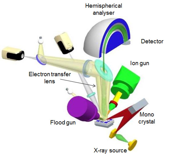
Figure 2. Schematic of an XPS system.
Development of XPS
XPS has matured as a technique. The increase in computing technology has been a contributing factor here.
Specialist applications have also evolved leading to increased analytical power and versatility of the technique. Examples include:
- Depth Profiling Uses an ion beam to etch away the surface exposing new layers which as analysed by XPS
- XPS Mapping Reveals the presence of chemistries across the surface any allows investigations of regions from tens ofmicrons across to several millimetres.
- XPS Parallel Imaging Similar to XPS mapping, it offers increased spatial resolution.
- Angle Resolved XPS Distinguishes different electrons from different depths in the surface of a sample
- Charge Compensation For the analysis of insulators
With improvements in computing power XPS is also becoming easier to use including features like automated calibration. Modern computers enable operators to carry out many tasks, often simultaneously resulting in greater analytical efficiency. These processes include manipulate samples automatically, acquire and process data and display and generate reports.
In line with increases in computing horsepower are memory increases. These allow databases of XPS spectra to be stored on board, with energy levels being automatically measured, overlapping peaks resolved and compositions determined. In addition, more in-depth analyses are also simplified such as generating depth profiles.
In parallel with these developments are improvements in the user interface. The user interface simplifies experimental setup, data collection and data analysis. In doing so, the whole process is streamlined making the technique more accessible to more users and operators, bringing the technique closer and more relevant to more people.
Depth Profiling and Gas Cluster Ion Sources
The ability to perform depth profiling adds another dimension to XPS analysis (pun intended). By alternating ion beam etching and XPS analysis, sub surface compositions, or the composition as a function of depth can be determined in a layer-by-layer fashion. This is particularly of interest for manufacturers of coated products, touchscreens, surface engineered components, multi-layered materials etc.
Traditionally monatomic Ar+ ions have been used to bombard the surface with energies ranging from a few hundred eV to several keV. It has been popular due to its relatively heavy atomic weight and inertness which makes it suitable for a large percentage of materials. This system is somewhat limited when investigating softer samples such as polymers where the Ar+ ions can damage the surface and sometimes alter the composition, hence distorting analyses.
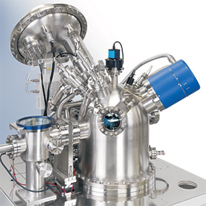
This problem has been overcome in recent times by Thermo Scientific who introduced the next generation MAGCIS dual mode ion source that can be operated as a monatomic or gas cluster ion source. Operators can switch between modes with the click of a mouse, and even use both modes in a single experiment.
MAGCIS is suitable for both depth profiling and cleaning or removal of surface contaminants and is especially useful for depth profiling materials that may consist of layers of organic and inorganic materials.
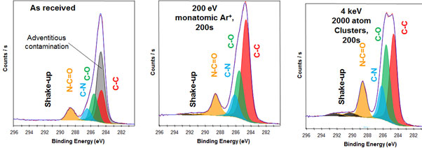
Figure 3. Polyimide which is prone to damage during etching. The middle spectra shows how the the chemistry is significantly affected by monatomic etching. The right side spectra shows how the chemistry is unaffected by cluster etching.
The gas cluster ion source utilises gas clusters of the nature Arn+ (50?n?2000). The gas cluster is much heavier, while still being able to remove material. However the beam energy is spread across the cluster. Upon impact with the sample, the gas cluster disintegrates dissipating energy laterally. This reduces damage to the sample, resulting in spectra that accurately represent the sample.
Ultraviolet Photoelectron Spectroscopy (UPS)
UPS was developed by David Turner from Imperial College (UK) in parallel to Siegbahn. It differs in that it determines molecular species and exhibits greater surface sensitivity compared to XPS with signals being generated by the outermost 2-3nm. In UPS, samples are exposed to UV photons generated by helium, (argon or neon) gas discharge lamps.
Due to the lower energy of the photons (compared to X-rays), spectra are generated by the valance band region leading to experiments relating to valence band acquisition and workfunction measurement.
Valence Band
Valence band data is typically used for materials characterisation through spectral fingerprinting. As many of the orbitals which are responsible for generating the valence band photoelectron signal possess a high degree of hybridisation and hence shifts in peak binding energy, these studies are typically performed on samples with well-known electronic structures or in conjunction with computational studies.
When in combination with XPS, the two data sets create a powerful tool for materials characterisation. UPS can be used to determine different electronic transitions and states using different photon energies.
Workfunction
The electronic workfunction is the difference between Fermi level and Vacuum level and is of particular interest to developers of electronic devices. Workfunction is stgrongly influenced by variations in composition or structure at the surface e.g. surface contamination. It is often used by designers of electronic devices who need to match valence and conduction bands in multilayered devices.
Current State of Play
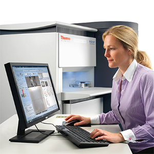
 XPS instruments have come a long way in the last 10 to 20 years. What was once the realm of specialist surface science is now breaching the mainstream. With developments in computing and other related technologies and techniques (such as MAGCIS and UPS) that can be integrated into XPS, XPS is becoming a more widely applicable materials analysis methodology. In fact, systems like the KAlpha+ from Thermo Scientific are also relatively affordable while offering high levels of throughput and sensitivity as well as features like remote access and operation. These systems bridge the gap between routine measurements and high end research. Increased levels of automation and user-friendly operator interfaces allow users of any level of expertise to generate research quality data with a minimum of time and effort.
This article was originally published in the April 2017 edition of Materials Australia magazine. XPS – Demystified by Dr. Cameron Chai.