
Melbourne Centre for Nanofabrication Adds Cutting Edge Nanolithography Capability
Nanotechnology is widely considered to be the way of the future for electronics, medicine and many other scientific endeavours. The ability to fabricate components with nanoscale features is extremely attractive as it will enable manufacturers to better control the structure and properties of the component more precisely, as well as being able to more easily fit them into tiny devices. This is the area that the Melbourne Centre for Nanofabrication (MCN) specialises, and will make great strides in, following the installation of a unique high resolution nanofabrication tool, the Nanofrazor, at the beginning of July.
With developments in nanotechnology happening so quickly, it is important for institutions like MCN to have access to cutting edge technologies and equipment. To this end, MCN have just commissioned a Thermal Scanning Probe Lithography (t-SPL) tool from SwissLitho that will allow them to create 3D nanodevices with features as small as 10nm.
The NanoFrazor was purchased through a LIEF (Linkage Infrastructure, Equipment and Facilities) grant from the Australian Research Council. The bid was led by Professor Ray Dagastine from the University of Melbourne with researchers from 5 university partners and CSIRO. Their goal was to establish a rapid 3D nano-scale prototyping capability at MCN, part of the Victorian node of the Australian National Fabrication Facility (ANFF). The ANFF is an NCRIS funded organisation devoted to providing Australian academic and industry researchers with open access micro and nanofabrication centres around the country.
This installation is significant as it is the first t-SPL installation in Australia and only the 6th in the world, giving Australia a technological advantage over many other developed nations. The technology itself is unique to SwissLitho, a company that was spun out of technology originally developed at IBM.
When asked about the new acquisition, Prof. Dagastine replied, despite the fact that NanoFrazor is such a new product, we were very comfortable knowing that it had evolved from IBM research and used scanning probe technology which earned them a Nobel Prize in 1986. We chose to install it at Melbourne Centre for Nanofabrication (MCN) as this is the largest open access research nanofabrication and cleanroom facility in Australia, providing the best access for the Victorian nanofabrication community.
t-SPL is the latest technology to become available for nanofabrication and offers many advantages over Electron Beam Lithography (EBL) technology – one of only a handful of techniques capable of creating structures at these scales – which has been around for over 50 years. t-SPL uses an extremely sharp computer controlled stylus to pattern surfaces by evaporation and decomposition, resulting in highly accurate features. This also means that there is no damage from high energy electron beams and processing does not need to performed in vacuum environments making the process much simpler and cheaper to run and takes up less space compared to EBL tools.
Another unique feature of the t-SPL approach, is the ability to precisely pattern in three-dimensions. One of SwissLithos more popular demonstrations of this is a nanoscale reproduction of their beloved Matterhorn.
Another key advantage of the t-SPL system is closed loop processing with in situ metrology. Using the same sharp probe, the NanoFrazor simultaneously measures and images the nanostructure allowing you to instantly check what you have created. This vastly speeds up the development process.
Access to this new technology opens up many possibilities for ANFF researchers said Prof. Saulius Juodkazis from Swinburne University, who was also key to the success of the bid. When asked about the potential for the technology, he identified some areas where it would be applicable. He said, the 3D capability of NanoFrazor to pattern resist materials is very appealing to the community working on flat-optical elements and phase masks. Other areas where I can see the Nanofrazor having an impact include patterning nano-membranes with sub-10nm nano-holes for water and gas sensing. My team in particular will be looking at ways to fabricate high-electron-mobility transistors (HEMTs) for use as emitters and detectors in the terahertz (T-ray) devices which has the potential to open up new applications in medical imaging.
AXT represents SwissLitho in Australia and New Zealand. For more information about the NanoFrazor t-SPL system click here.
Posted July 28, 2016
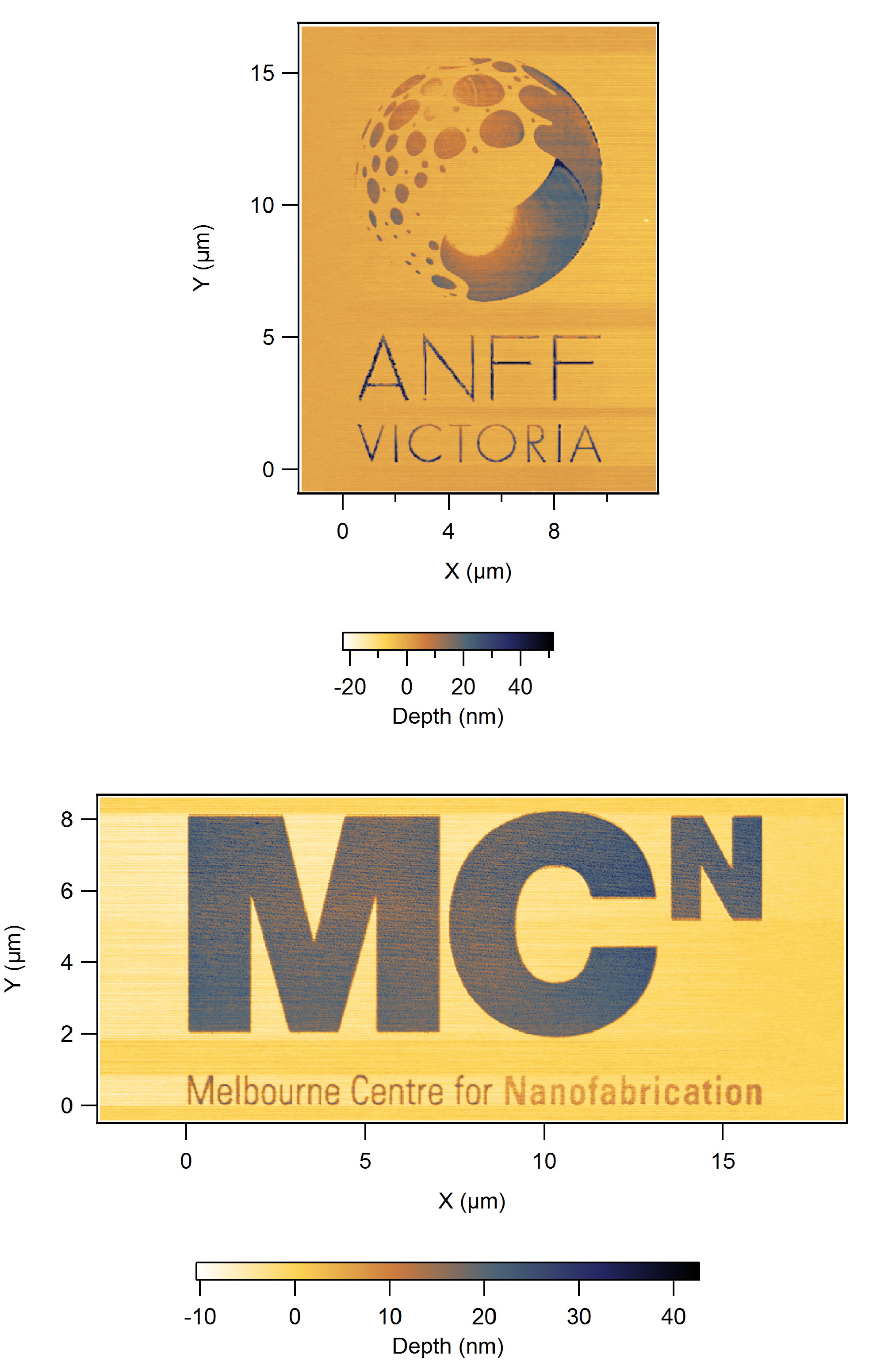
ANFF and MCN Logos patterned using the SwissLitho Nanofrazor.
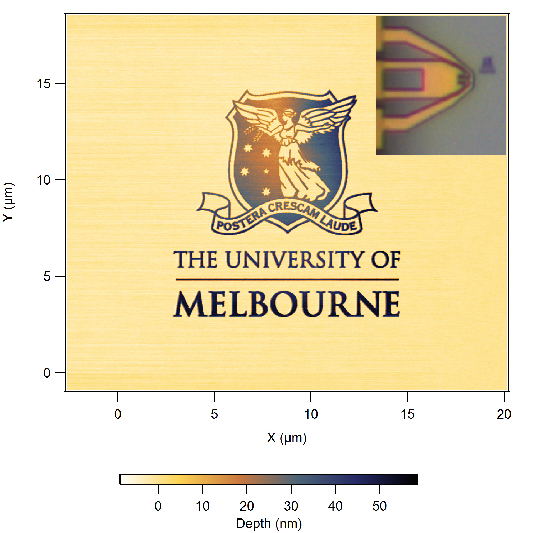
University of Melbourne logo patterned using the SwissLitho Nanofrazor.