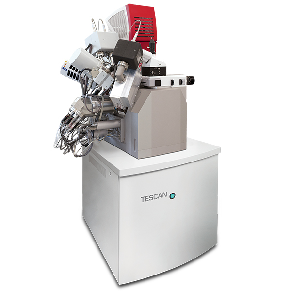
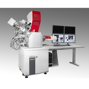
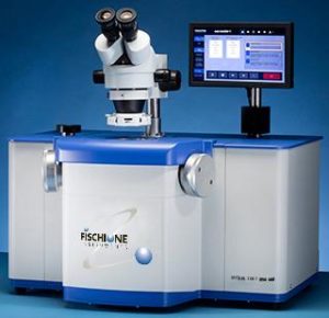
GAIA – Ultra-High Resolution SEM with Focussed Ion Beam UHR SEM/FIB
The TESCAN GAIA harmoniously marries an ultra-high resolution SEM column with Triglav technology a high performance FIB column within a single chamber. The Field Emission FE-SEM column offers excellent resolution at low voltages, along with stunning mage quality in SE and BSE modes across the entire energy range. As the third generation, it benefits from development and upgrades to previous generation instruments. Examples include faster electronics and more powerful computing that speed up analytical and imaging operations, as well as improving sample control.
FIB Column
The COBRA FIB is an ultra-high resolution column with class-leading (guaranteed) 2.5nm resolution. It is the sharpest FIB in its class which results in the highest levels of resolution for both imaging and milling, making it suited to nanoengineering applications.
It is capable of producing sub-2nm images with gallium at 1pA. The column has also been optimised for high current modes offering a tightly defined beam shape for high precision milling. Furthermore, a fast cross-section milling technique increases milling time by 2.5 times.
GAIA is also capable of depositing conducting and non-conducting materi9als, as well as enhanced and selective etching using either the electron beam or ion beam in conjunction with highly flexible gas injection technology. This also enables high precision control over the milling process.
Novel FE-SEM Column
The GAIA UHR SEM column now incorporates Triglav® technology which affords you sub-nanometer resolution. and increased stability. The system really shines when it comes to imaging at extremely low accelerating voltages making it an idal choice for sensitive materials such as integrated circuits, biological specimens and other life science studies.
Key Features
- Extraordinary SEM resolution with single pole 60° objective lens
- Best-in-class range of display modes (Field, Resolution and Depth) leveraging off TESCANs unique Wide Field Optics
- Simultaneous SEM imaging during FIB milling or deposition
- High sample manoeuvrability using a motorise compucentric stage
- Field-free mode for working with magnetic samples
- High probe current (up to 200nA for SEM)
- EBL (Electron Beam Lithography) with ultra-short dwell times, as low as 20ns
- Ultra-high FIB resolution and superior performance using the probe current
- Powerful DrawBeam toolbox featuring basic and advanced programmable objects with selectable process parameters
- Extraordinarily high number of ports for a range of detectors
Triglav Technology
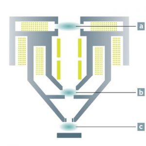
TriLens objective system. (a) IML, (b) Analytical lens, (c) UH-resolution lens
TESCAN have upped the ante with the release of their next generation Triglav® Ultra-High Resolution (UHR) SEM column. Thanks to the TriLens and EquiPower technologies, users can achieve sub-nanometer resolution down to 0.7nm at 15keV and an impressive 1nm at 1keV making it ideal for imaging nano-sized features.
Triglav provides you with improved imaging and analytical capabilities while also providing enhanced surface sensitivity and image contrast at the extremely low beam energies. Triglav columns are now standard on TESCANs range of UHR SEMs including the
- XEIA (Xe Plasma FIB-SEM)
- GAIA (Ga FIB-SEM)
- MAIA (FEG-SEM)
The higher performance and improved imaging of these systems can be attributed to unique electron optics and a robust detection system. The new column includes the TriLensTM (three objective lenses) and TriSE/TriBSE (3 SE and 3 BSE detectors) mated together resulting in different imaging modes to suit your specific requirements.
The Triglav column incorporates three SE and angle-selective BSE detectors providing maximum surface and compositional contrast. Additionally, the chamber has been redesigned to cater for larger samples.
EquiPower technology introduces new levels of beam stability. While this technology will benefit imaging operations, it really comes to the fore with time consuming operations such as FIB milling and automated TEM lamellae preparation.
Software
The GAIA employs TESCANs well-known and user friendly software package for both instrument control and analysis. It features functions including:
- Automated operation of many routine operations and setup procedures
- Remote access to monitor the instrument and controlling measurements
- Scripting libraries for customisation and further automation
- Further levels of customisation available to experienced users
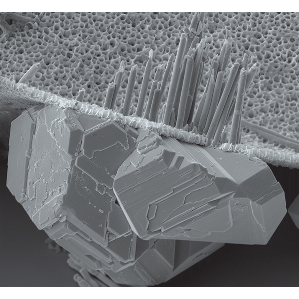
Applications
Materials Science
- Analysis of difficult to image samples such as non-conductive materials, magnetic materials and samples with charge compensation
- Patterning of complex nanostructures and high resolution imaging
- Highly analytical platform with the ability to add additional systems such as 3D EBSD/EDS, WDS, TOF SIMS, SPM and confocal Raman microscopy
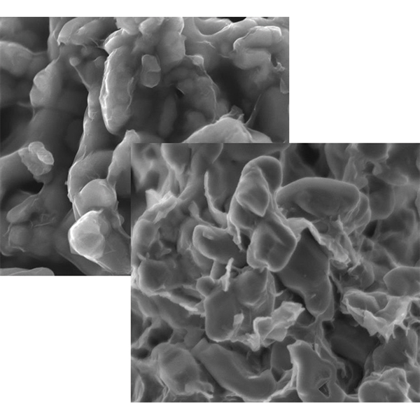
Life Science
- Investigating cell morphology, development of biocompatible materials, tissue engineering, microbiology etc.
- Variable pressure modes enable observation using tomography, Correlative Light and Electron Microscopy (CLEM) as well as cryo SEM/cryo FIB techniques
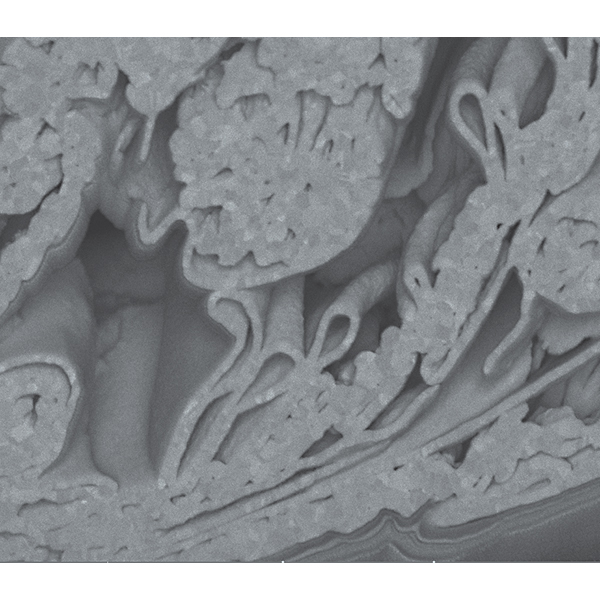
Semiconductors
- Prototyping with extreme accuracy using Ion Beam Lithography (IBL)
- Failure analysis of integrated circuits and layered structures
- Milling and deposition of small specific structures using a combination of FIB and Electron Beam Lithography (EBL).