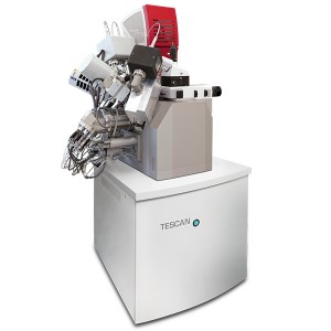
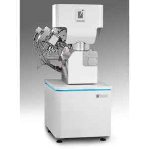
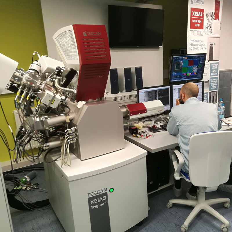
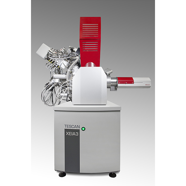
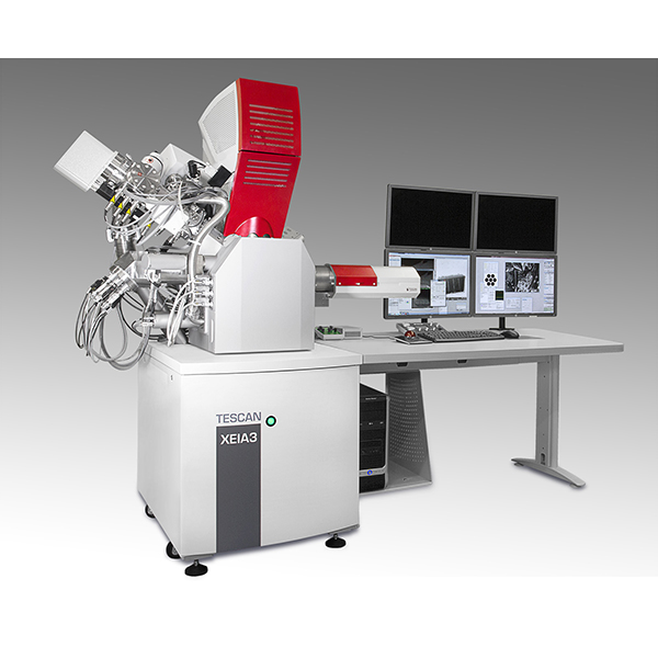
Xenon Plasma FIB Focussed Ion Beam with Ultra-High Resolution SEM UHR SEM/i-FIB
The XEIA3 is TESCAN’s flagship instrument combining the world’s sharpest Xenon plasma FIB (Focussed Ion Beam) column with an Ultra-High Resolution (UHR) SEM column. The marriage of these systems enables you to perform the most challenging milling and materials removal operations at speeds not previously possible with the highest levels of precision. This turn key solution opens up new possibilities in terms of research and applications.
The UHR SEM/i-FIB combination is well suited to high-throughput microanalytical applications. High milling rates matched with rapid data acquisition allows speedy analysis of large volumes of sample in short time frames. This, analyses such as 3D EDX and 3D EBSD becomes a simple operation and precise TOF-SIMS analysis becomes a a routine operation.
Xenon Plasma FIB
Most conventional FIBs use Liquid Metal Ion Source (LMIS) such as a gallium (Ga) ion source. Ga FIB’s deliver a small spot size, with performance dropping off at high currents (>10nA) and spot size increases making them unsuitable for large volume milling. The Xe plasma ion source FIB overcomes this limitation with much higher beam currents possible, resulting in far greater rates of materials removal. Furthermore, the Xe plasma FIB has a superior lifetime and current stability.
Example: Using a Xe plasma FIB can perform a milling polishing task in 30 minutes compared to 40 hrs for a Ga FIB. Furthermore, the Xe plasma FIB ion flux is more consistent with excellent spatial uniformity which is suited to automated, precision milling.
Ultra-High Resolution SEM
The XEIA is now equipped with Triglav® technology providing you with sub-nanometer resolution and increased stability. The XEIA excels when it comes to imaging at low accelerating voltages. This makes it especially suited to imaging sensitive materials such as integrated circuits, biological specimens and other life science studies.
Key Features
- Powerful ultra-high resolution SEM column equipped with a high brightness Schottky emitter for high currents, low-noise and extraordinary imaging
- In-Beam detectors for excellent imaging at low energies and very short working distances
- Ultra-fast xenon plasma ion source FIB – high beam currents for outstanding milling speeds and an excellent performance in sputtering large volumes of material, and low beam currents for smooth polishing.
- Less implantation, doping or degradation of insulator deposition, a valuable feature for semiconductor industry
- Simultaneous SEM imaging during FIB milling or deposition (the whole process can be observed directly)
- Unique and advanced TESCANs technologies in terms of automated operations such as the In-Flight Beam TracingTM designed to accurately compute and adjust all the optimal parameters for high resolution imaging
- Advanced patterning and 3D characterisations capabilities powered by DrawBeam, a pattern editing tool that also provides real-time visualisation during milling or lithographic processes
- High-performance electronics for faster image acquisition up to 20 ns/pxl, an excellent deposition rate and ultra-fast scanning
- Novel solution for fast 3D microanalysis such as 3D EDX and EBSD reconstructions
- 12, 8 and 6 wafer inspection by means of an extended chamber – an exclusive TESCAN feature
- Unique integration with TOF-SIMS
- Gas Injection System (GIS) for enhancing your FIB applications
- Powerful turbomolecular and dry fore vacuum pump for keeping the chamber clean. Electron gun pumping by ion getter pump in ultra-high vacuum
Triglav Technology
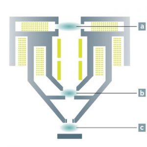
TriLens objective system. (a) IML, (b) Analytical lens, (c) UH-resolution lens
TESCAN have upped the ante with the release of their next generation Triglav Ultra-High Resolution (UHR) SEM column. Thanks to the TriLens and EquiPower technologies, users can achieve sub-nanometer resolution down to 0.7nm at 15keV and an impressive 1nm at 1keV making it ideal for imaging nano-sized features.
Triglav provides you with improved imaging and analytical capabilities while also providing enhanced surface sensitivity and image contrast at the extremely low beam energies. Triglav columns are now standard on TESCANs range of UHR SEMs including the
- XEIA (Xe Plasma FIB-SEM)
- GAIA (Ga FIB-SEM)
- MAIA (FEG-SEM)
The higher performance and improved imaging of these systems can be attributed to unique electron optics and a robust detection system. The new column includes the TriLensTM (three objective lenses) and TriSE/TriBSE (3 SE and 3 BSE detectors) mated together resulting in different imaging modes to suit your specific requirements.
The Triglav column incorporates three SE and angle-selective BSE detectors providing maximum surface and compositional contrast. Additionally, the chamber has been redesigned to cater for larger samples.
EquiPower technology introduces new levels of beam stability. While this technology will benefit imaging operations, it really comes to the fore with time consuming operations such as FIB milling and automated TEM lamellae preparation.
Materials Science
The Xe plasma source provides great advantages for making the most of chemical and compositional analytical techniques such as energy and wavelength dispersive X-ray spectroscopy, large scale 3D EDX and 3D EBSD reconstructions as well as full integration with TOF-SIMS for achieving superior resolution in surface analysis. XEIA3 is an extraordinary robust analytical platform with far reaching research potential in materials science.
Typical applications include:
- Research in new materials and their characterisation
- Study of non-conductive materials such as crystals, ceramics and polymers
- Patterning of complex nanostructures
Examples
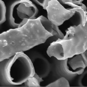
TiO2 nanotubes imaged at 1 keV with the
SE (BDM) detector.
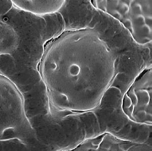
Fullerene imaged at 1 keV with the In-
Beam detector
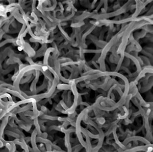
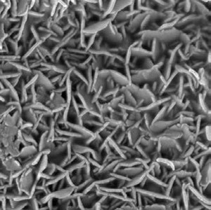
Carbon nanotubes imaged at 2 keV with
the SE (BDM) detector.
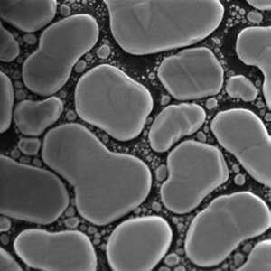
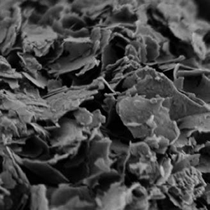
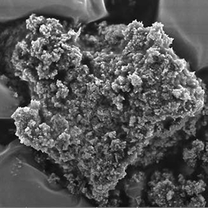
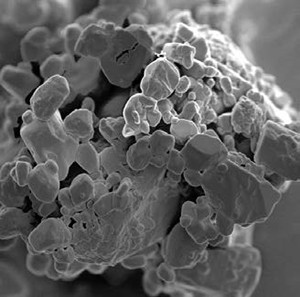
Golden grains on carbon imaged at 1 keV
with the SE (BDM) detector.
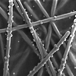
Ag wires imaged at 1 keV with the In-
Beam detector.
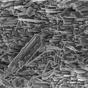
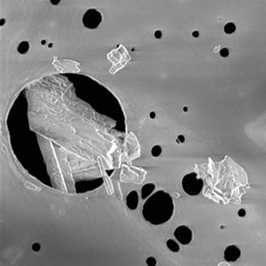
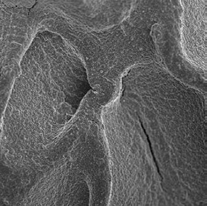
Cross-section surface on silicon imaged
at 2 keV with the SE (BDM) detector.
Ag electrode imaged at 2 keV with the
In-Beam detector.
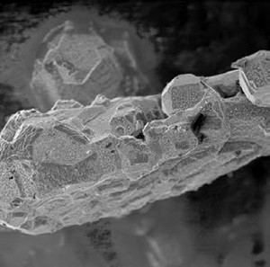
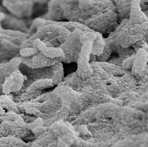
Hydroxyapatite biomaterial imaged at
5 keV with the In-Beam detector.
Life Sciences
XEIA3 superb imaging capability is designed for imaging a wide variety of sensitive biological samples in their natural state. This represents a great advantage as no coatings or chemical
fixing of these types of samples are needed, which makes the whole analysis process much simpler.
Typical applications include:
- Microbiology
- Biomedical engineering??
- Cell and tissue biology??
- Cellular analysis??
- Pharmaceutics??
- Study of dynamic processes such as crystallization or dissolution of substance??
- Study of particle properties such as the particle size, porosity, structure and contaminants
Examples
Pollen imaged at 2 keV with the In-
Beam detector.
Lamella from a peptide imaged at 5 keV
with the In-Beam detector.
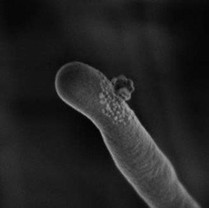
Mold fiber imaged at 800 eV with the
In-Beam detector.
Peptide imaged at 700 eV with the
In-Beam detector.
Pharmaceutical powder imaged at 2 keV
with the In-Beam detector.
Crop imaged at 2 keV with the In-Beam
detector.
Biomaterial imaged at 2 keV with the
In-Beam detector.
Mouse brain tissue imaged at 3.1 keV
with the In-Beam detector.
Semiconductors and Microelectronics
The powerful Xe plasma ion column makes XEIA3 the system of choice for the semiconductor and microelectronic industry. High currents for rough milling, ideal for lamellae preparation or large
cross sectioning; medium current for polishing and reducing surface artifacts (curtaining effect); small current for fine polishing of cross sections and lamellae.
Typical applications include:
- Trough-Silicon-Vias (TSV) analysis??
- Integrate Circuits (IC) and Microelectromechanical Systems (MEMS) and Failure Analysis??
- IC inspection and editing??
- 3D Tomography of Integrated Circuits??
- Solar cells inspection and efficiency analysis??
- Electron and Ion Beam Lithography??
- Nano-prototyping??
- In-situ lamellae imaging with the STEM detector
Examples
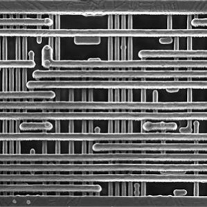
Metal deposition for circuit editing, image
taken at 5 keV with the In-Beam detector.
Detail of the cross-section in an IC
device imaged at 2 keV with the In-
Beam detector.
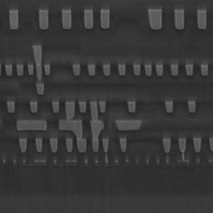
Detail of a cross-section of an IC imaged
at 5 keV with the In-Beam SE detector
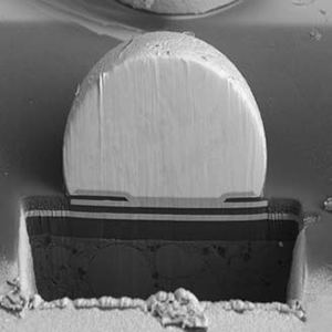
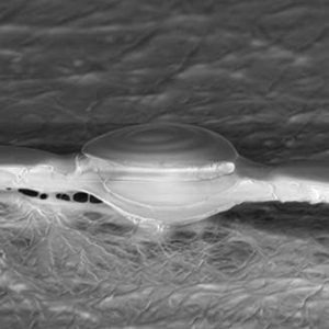
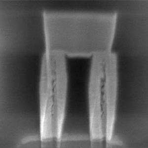
Cross-section of a solder bump imaged
at 10 keV with the BSE detector
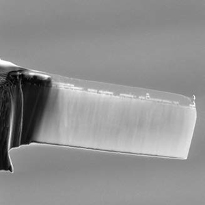
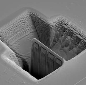
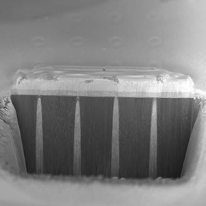
Large TEM lamella prepared with Xe
plasma FIB and the Rocking Stage,
imaged at 10 keV with the SE detector.
Detail of the cross-section in a solder
bump connection for inspection purposes.
The image was taken at 10 keV
with the In-Beam BSE detector.
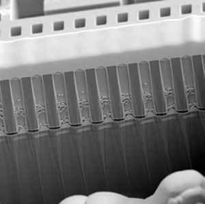
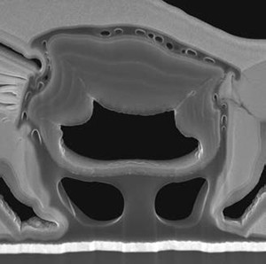
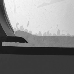
Cross-section of a storage device
component imaged at 5 keV with the
In-Beam detector.
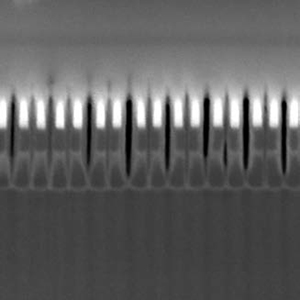
LCross-section of TSV imaged at 3 keV
with the In-Beam detector.